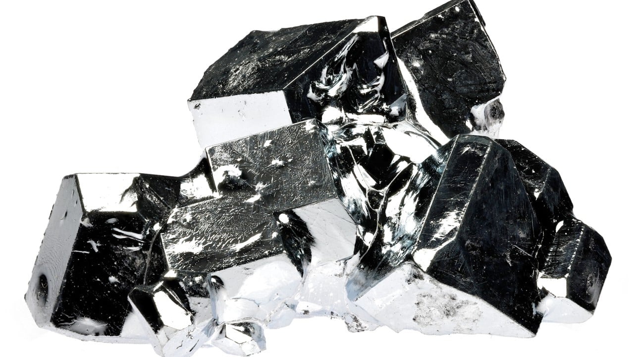
Compared to widely used wide band gap materials, such as gallium nitride and silicon carbide, gallium oxide has significant performance advantages. However, it has been notoriously difficult to process.
03:36
China restricts critical metal exports following Western semiconductor curbs in latest trade war
China restricts critical metal exports following Western semiconductor curbs in latest trade war
In August last year, the US Commerce Department’s Bureau of Industry and Security imposed an export ban on advanced semiconductors, including gallium oxide, citing national security concerns.
Advertisement
Gallium oxide allows “semiconductors to work under more severe conditions, such as at higher voltages or higher temperatures. Devices that utilise these materials have significantly increased military potential”, said Alan Estevez, commerce undersecretary for industry and security, in a Reuters report.
The ban seemed to aim at hindering China’s participation in next-generation semiconductor competition, but has proven ineffective.
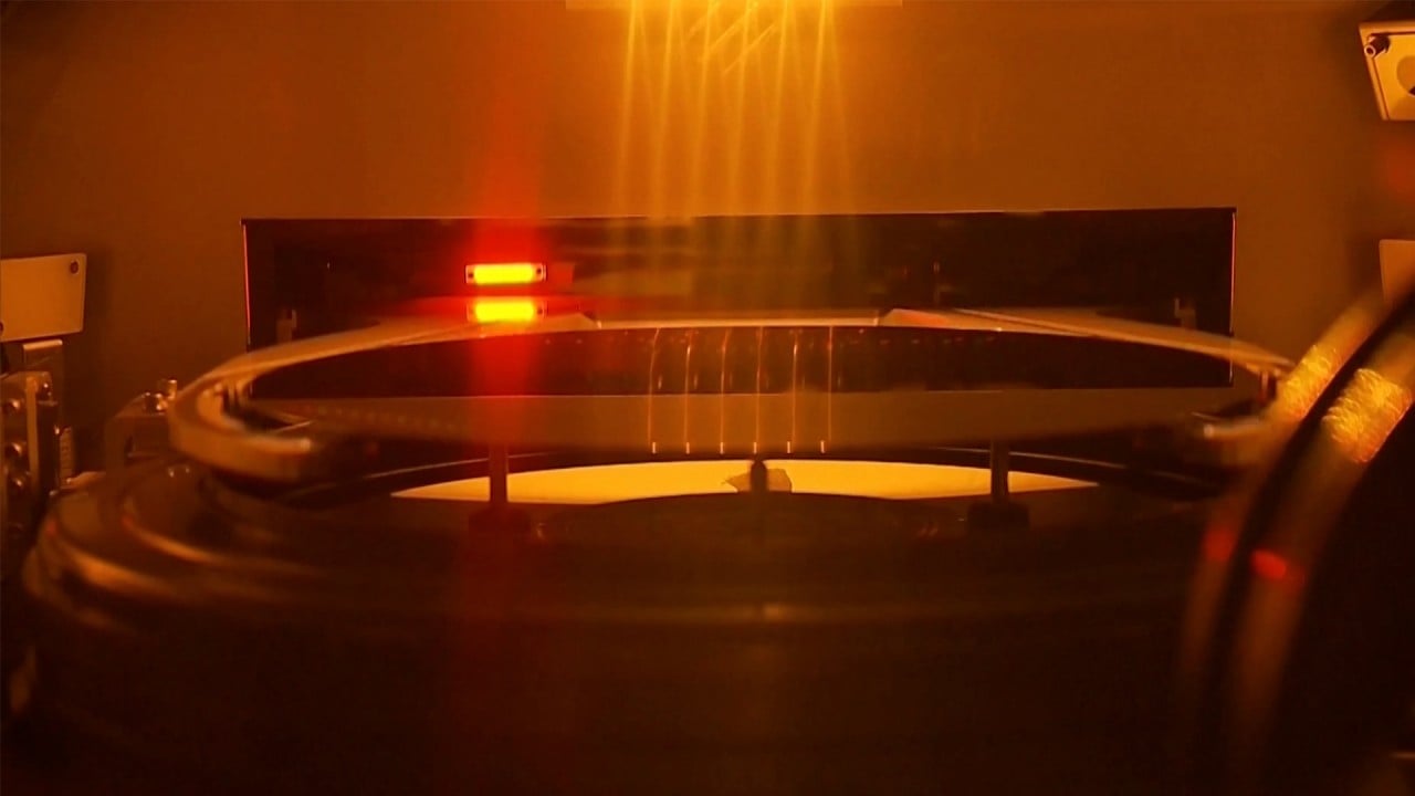
A team from Zhejiang University has made strides using a self-developed approach. Led by Yang Deren, a member of the Chinese Academy of Sciences and director of Zhejiang University’s State Key Laboratory of Silicon Materials, the team produced 4-inch wafers in August, improving on their 2-inch wafers from May last year. Moreover, their process is more simple, controllable and cost effective.
Advertisement
“We are determined to meet national needs for semiconductor materials and break the bottleneck through technological innovation,” said Professor Zhang Hui from the team in an interview with the Science and Innovation Daily in May.
Chinese controls on gallium to have ripple effects on country’s exporters
Chinese controls on gallium to have ripple effects on country’s exporters
Zhang found that for third generation and beyond wide band gap semiconductor materials, most are synthesised through vapour-phase methods. In contrast, gallium oxide is the only material that can form single crystals by solidifying from a melt at standard atmospheric pressure, helping to cut fabrication costs and thus aid mass production.
Advertisement
“In Japan and America, a modelling method is commonly used. However, this method requires a large amount of iridium to make the crucible. Typically, a 4-inch gallium oxide crucible would need at least 5kg [11lbs] of iridium,” he said.
“Given that the price of iridium is almost three times that of gold, the method significantly increases the cost of gallium oxide. Moreover, a foreign method could potentially lead to international intellectual property disputes,” Zhang said.
02:55
US Senate passes Chips and Science Act to compete with China’s semiconductor industry
US Senate passes Chips and Science Act to compete with China’s semiconductor industry
In contrast, the casting method proposed by Yang reduces iridium use by 80 per cent, significantly lowering production costs. The process is also relatively simple and shorter, making it suitable for automated control and aiding future industrialisation.
Advertisement
Zhang established the Garen Semiconductor Company in Hangzhou in September last year and focused on developing gallium oxide materials.
The team has currently applied for multiple domestic and international patents and plans to further optimise its casting method.
“By controlling the temperature gradient during crystal growth, we aim to produce larger-sized gallium oxide single crystals,” Zhang said.
China quietly poaches chip talent from elite US universities
China quietly poaches chip talent from elite US universities
A Beijing-based private firm, MIG Semiconductor Company, successfully produced 4-inch gallium oxide wafers in December. The company is also building China’s first integral production line, combining crystal growth, processing and performance testing. The construction is expected to be completed by the end of the year, according to its website.
Advertisement
In general, gallium oxide semiconductors offer advantages in high-voltage resistance, their smaller size, and less energy consumption in power transmission. They are used in communications, radar, aerospace, high-speed trains and electric vehicles.
“By 2025, the market for gallium oxide devices will begin to surpass that of gallium nitride, reaching US$1.542 billion by 2030,” according to an estimate by Japanese company FLOSFIA.
Advertisement


