The work was the first universal approach to 3D-printed semiconductors and other inorganic functional materials with nanoscale resolution, a process that could pave the way for new advances in semiconductor device manufacturing, the researchers said.
The study, co-led by associate professor Zhang Hao, and professors Li Jinghong, Lin Linhan and Sun Hongbo – all from Tsinghua University – was published in the peer-reviewed journal Science on September 28.
The new approach – dubbed “3D Pin” – involved forming semiconductor nanocrystals that were suspended in a specially designed colloidal ink. The team then added a molecular “glue” to the ink that, when laser activated, formed stable bonds between the nanocrystals, resulting in robust 3D structures.
02:03
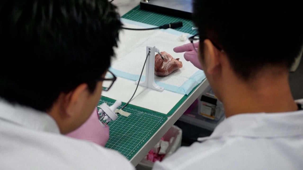
Robot prototype 3D prints biomaterials inside human body, lowering surgical risks
Robot prototype 3D prints biomaterials inside human body, lowering surgical risks
Because of the versatility of the ink formula, the method could be used to create various types of semiconductors, metals and semiconductor oxides, and could even create mixed and heterogeneous structures, the researchers said.
“The method enables high-resolution 3D printing without altering the inherent qualities of the semiconductor crystals,” said Marc S. Lavine, editor of Science.
The materials printed using 3D Pin had high purity content, with a mass fraction of inorganic components greater than 90 per cent. That compared with materials produced through traditional methods using printing templates or adhesives, where it is difficult to exceed 50 per cent of the inorganic mass component.
3D Pin can achieve a printing resolution of 150 nanometres, which means it can print precise, complex three-dimensional structures, such as human faces, flowers or even the Eiffel Tower.

Compared to traditional integrated circuit manufacturing techniques, which are two-dimensional, 3D Pin can create three-dimensional structures directly without stacking layers. “Our method has the potential to be a more cost-effective alternative for making semiconductor devices with 3D structures,” Zhang Hao said on Sunday.
The technology is not intended to replace current integrated circuit production, but rather to supplement it, particularly for devices requiring 3D structures, Zhang said.
By printing periodically arranged quantum dots with different optical properties, a pixel array could be formed to achieve a three-dimensional high-definition display, according to the researchers.
In a visual representation accompanying the paper, the team showed the technology’s capabilities by 3D-printing a dragon-shaped pixel array in red and blue semiconductor crystals, which glowed pink when lit up together.
To out-compete China, Biden launches 3D printing initiative
To out-compete China, Biden launches 3D printing initiative
Since the printed structures contain both inorganic components and organic glues, the structures printed by 3D Pin can be more durable than pure inorganic materials, the researchers said.
For example, 3D Pin can print ordered bionic structures like mussel shells, which contain both inorganic salts such as silicon oxide, as well as calcium carbonate and some protein molecules.
“The printed structures preserve the intrinsic properties encoded in the nanocrystals and also show additional functionalities stemming from their 3D geometries,” Zhang said in the paper.
The research team’s future goals include refining the purity of the inorganic components to as close to 100 per cent as possible, and improving optical technology to enhance printing precision, speed and other properties.

